


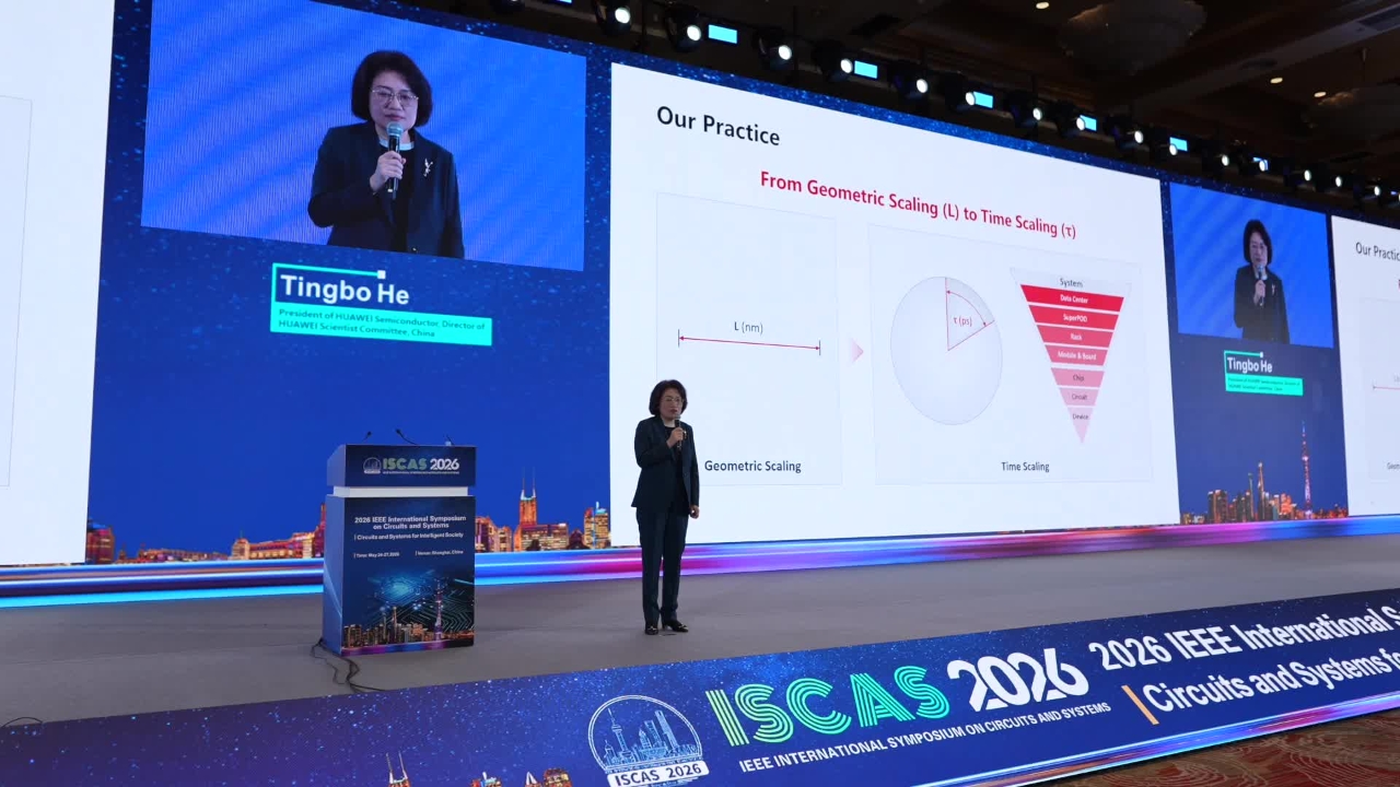
He Tingbo, Huawei board member and president of its semiconductor business, delivered a keynote speech titled "New Semiconductor Path in Practice" at the 2026 IEEE International Symposium on Circuits and Systems (ISCAS) held on Monday.
In her speech, she presented the Tau (τ) Scaling Law, a new principle for guiding the future development of the semiconductor industry.
This law proposes replacing geometric scaling with time (τ) scaling as a new guiding principle for the evolution of both semiconductors and electronic systems.
Based on this principle, innovative technologies such as LogicFolding can be used to continuously compress signal propagation delay and steadily improve transistor density, which will drive the ongoing evolution of semiconductors and electronic systems.
Based on the Tau Scaling Law, Huawei has developed innovative core technologies like LogicFolding and established a multi-level co-optimization mechanism that spans semiconductor devices, circuits, chips, and systems.
This mechanism aims to systematically shorten the time constant τ in order to drive up performance, energy efficiency, and transistor density at each level.
By 2031, the high-end chips Huawei designs based on the Tau Scaling Law are expected to feature a transistor density that is equivalent to 14 Å (1.4 nm) processes.
Looking ahead, He noted, "We believe that openness and collaboration are key to driving ongoing progress in the semiconductor industry. No single company can independently find all the answers along the path of semiconductor evolution. With the τ Scaling Law, we look forward to working closely with scientists, engineers, and industry partners around the world to drive the sustainable development of the semiconductor and electronics industries."

































 京公网安备 11010202009201号